The problem we set out to solve
Renewable sources such as photovoltaic panels and fuel cells often produce a voltage that is far too low to be directly useful. Raising it to the level required by a grid, inverter, or DC bus can demand an exceptionally large boost—the territory of high-gain DC-DC converters.
Most approaches to achieving that gain come with significant tradeoffs:
- Stacked diode-capacitor or voltage-multiplier stages can reach high gain, but the growing component count reduces efficiency and reliability while adding cost and bulk.
- Two-stage and multistage designs can produce impressive gains, but often increase switch-voltage stress and reduce efficiency.
- Some switched-capacitor designs require very large duty cycles and, without proper input filtering, draw high-ripple current that is harmful to photovoltaic panels and fuel cells.
- Designs with additional switches can manage voltage stress, but narrow the usable duty-cycle range and complicate control.
- Several alternative topologies offer soft switching but cannot achieve enough gain for demanding step-up applications.
We wanted a single-stage converter that could reach ultra-high voltage gain, keep source current smooth and continuous, and limit semiconductor voltage stress without accumulating a large number of components.
The core idea
The proposed converter combines a single two-winding coupled inductor, a voltage multiplier cell, and a passive clamp circuit while using only two power switches.
- The gain is quadratic, not linear. Instead of scaling roughly as 1/(1-D), the output voltage scales approximately as 1/(1-D)2. Gain therefore rises much faster with duty cycle, allowing a very high output voltage without pushing the converter to an extreme duty cycle.
- One coupled inductor does the heavy lifting. A two-winding coupled inductor is simpler and more compact than a three-winding design, with lower magnetic complexity and leakage inductance while retaining useful turns-ratio flexibility.
- The switches see only a fraction of the output voltage. The multiplier cell clamps both switch voltages to levels governed mainly by input voltage and duty cycle, enabling lower-voltage-rated and potentially lower-cost MOSFETs.
- The output diode turns off cleanly. Current reversal in the coupled inductor and recycling of leakage energy through the clamp diodes allow the output diode and one internal diode to turn on and off under zero-current conditions, reducing reverse-recovery loss.
- Input current remains continuous. A front-end input inductor keeps source current smooth and low-ripple, supporting both efficiency and source lifetime.
An honest limitation
The output diode and one internal diode achieve soft switching, but the power switches themselves do not turn off softly in this design. Improving that behavior remains an opportunity for future work.
What we built and tested
A 425 W prototype was built and operated at 100 kHz from a 30 V input. An analog TL494-based controller generated the switching pulses.
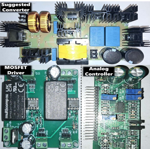
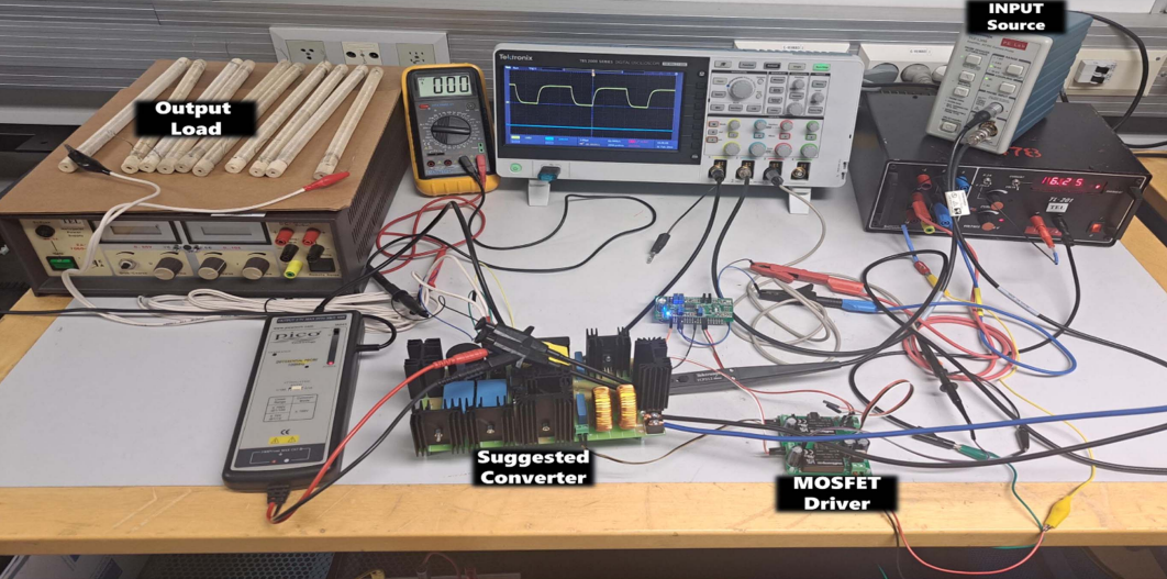
- The two switches reached peak voltages of only 63 V and 191 V, respectively—far below the several-hundred-volt output—confirming the multiplier cell’s clamping action.
- The internal diodes blocked approximately 88 V each, while the output diode blocked approximately 490 V, closely matching the theoretical equations.
- Diode D3 turned off at zero current because leakage energy was recycled instead of dissipated, demonstrating the intended soft-switching behavior.
- During output-load steps between approximately 475 W and 294 W in both directions, the controller maintained output-voltage regulation.
- A detailed loss breakdown produced an overall efficiency of 95.40% at 425 W, with the switches and diodes responsible for most of the losses.
Why this matters
Compared with a broad group of recently published high-gain topologies, this converter delivered the highest voltage gain for a given duty cycle while keeping the combined voltage stress on its switches and diodes below most alternatives—all with two switches and one coupled inductor.
As more low-voltage renewable sources must connect to grid interfaces, DC microgrids, and storage systems, a compact single-stage converter that reaches serious operating voltages without cascaded stages or a large component count offers a practical path to simpler, more efficient power conversion.